

Advanced Packaging
Piecing Together the Future

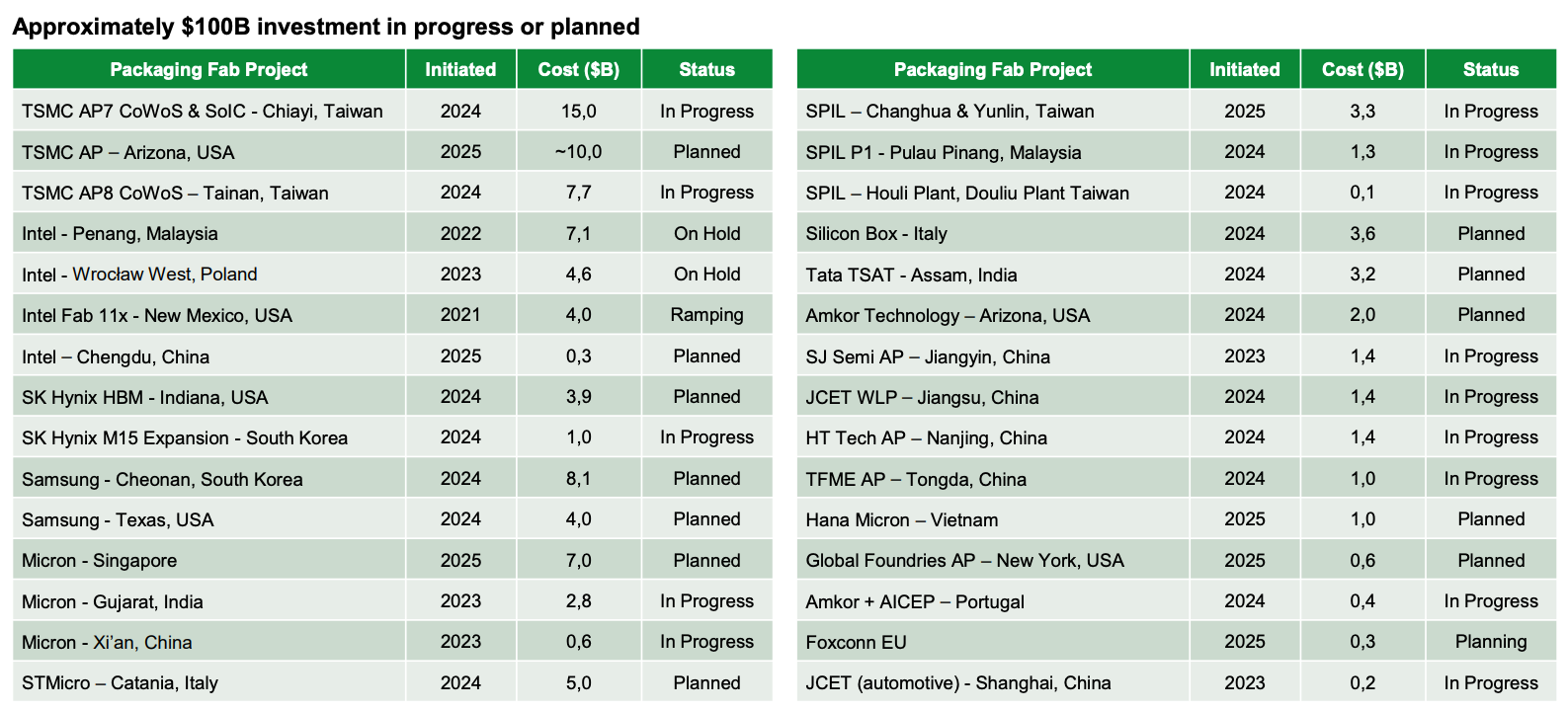
The mechanics here are complex, but this will be one of the most transformative developments in AI. Nearly $100B of investment has been made into a few companies, and the portfolio we have put together is positioned to capitalize on this.
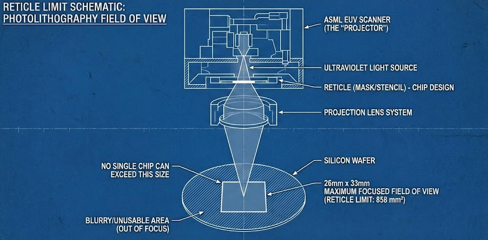
When Nvidia launched the Hopper H100 back in 2022, it was the most powerful chip at the time, with 80 billion transistors. What’s more interesting was the size of the chip — 814 square mm. This number is important as it was very close to the Reticle Limit of 858 square mm.
The Reticle Limit is simply the area within which the current chip-printing machines can focus without causing errors. It has been the industry standard for roughly 35 years because a larger lens would be significantly heavier and more prone to blurring during chip printing.
With the Nvidia H100 chips already using 4nm transistors and an 814 square mm chip size, the only way to double the number of transistors for the next model was to reduce the transistor size to 2nm. Instead of waiting around for a reliable 2nm process1, Nvidia used Advanced Packaging to glue together two of the largest possible chips to make the Nvidia Blackwell (B200). Blackwell had a mind-bending 208 billion transistors, more than doubling the H100 transistor count.
While making chips faster by shrinking them has been our go-to solution for the past 50 years, we might be approaching the limit of how small an individual transistor can be. Without getting into the nuances, as you approach 2nm and beyond, you have to spend exponentially more in manufacturing costs and cooling solutions. That’s why companies are betting more on Advanced Packaging.
How much more?
Approximately $100 billion in investment has flowed into the field over the last 3 years.
Market Sentiment dives deep into the bottlenecks of the AI world. Join 64,000 other investors to make sure you don’t miss our next briefing.
Advanced Packaging
The following section is highly simplified, but it should provide clarity on how Advanced Packaging is addressing a critical bottleneck. Anyone who has ever assembled a PC knows that all components are mounted on a motherboard and connected via PCBs (as shown below).

The problem here is two-fold. One is that CPUs are considerably faster and spend 90% of their time waiting for data to arrive from RAM. The second is that moving data over long distances requires high voltage, which increases overall power consumption. Both issues are resolved using Advanced Packaging. Instead of assembling components in 2D, we now stack them on top of each other.
Since the memory now sits on top of the processor, there is no delay in accessing data from memory, and the operation becomes much more efficient [as seen in the video below].
With Advanced Packaging, we are solving two of the biggest problems in chip design:
First, we can now join multiple chips and make them behave like one, keeping Moore’s law intact for a little longer.
Secondly, since we are able to mount memory right on top of the processor, we make the data transfer significantly faster. A traditional DDR5 RAM reaches speeds of up to 70 GB/s, whereas with Advanced Packaging, you can hit 1,200 GB/s.
Why now?
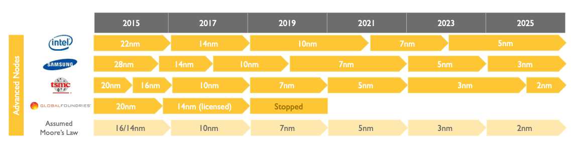
As we highlighted in the beginning, the go-to solution for building faster chips was to cram more transistors into the same chip. This has worked out well, and over the past decade, we have reduced transistor size from 22nm in 2015 to 2nm by 2025. But this reduction has been achieved at exponentially rising costs, with 2nm chips 10x more expensive in both design and manufacturing than in 2015.
The costs are so high that only 3 companies in the world are currently developing 2nm technology: Intel, TSMC, and Samsung. The optimal solution to rising costs (as shown by Nvidia) is to use older 4nm technology and leverage Advanced Packaging to connect multiple chips to act like one.
Building an Advanced Packaging Portfolio
As promised last week, we will be launching the Market Sentiment portfolio by investing in a basket of stocks positioned to benefit from the rise of Advanced Packaging. This sector is expected to grow between 30 to 40% CAGR for the next 5 years, and the total market is expected to cross $100B by 2030.
To put this in perspective, only 3 players use Advanced Packaging to create High Bandwidth Memory and own 100% of the market. The demand for this technology is so high that these $100B+ companies have tripled in the last 6 months.
Let’s dig in: